I’m new to this forum and currently working on a Anti-spark switch for my boards.
All the available projects didn’t fit my needs, so I decided to design my own switch.
In my opinion, they all were too big, or too expensive or didn’t have the feature I needed.
maximum current of around 200A (more with additional copper and cooling)
maximum voltage of 60V
12V 50mA LDO output
controlled dI/dt with capacitor and current limiting resistor
two IRFS7530 N-channel MOSFET
BQ76200PWR High Side MOSFET Driver
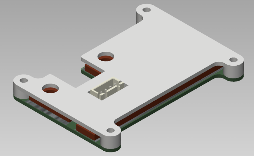
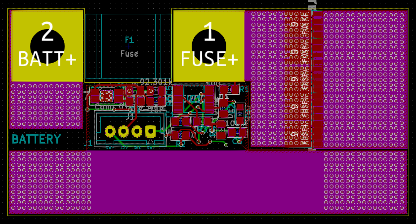
A holder for a LittleFuse BF1
4 pin JST XH connector for an external switch
exposed pcb traces to add solder or a copper bar for lower resistance
LDO
The 12V LDO is only used to drive an LED that is included in my switch. It won’t deliver much current, due to the high heat dissipation: 38V delta voltage means 0.38W for every 10mA, which is much for such a small package.
You can leave it unused if you want.
FUSE
As seen by other Anti-Spark switches I went with the LittleFuse BF1. It can be soldered directly to the PCB, so there is no need of screw terminals. However, there are 6.5 mm screw holes. You can also use a copper strip in replacement for the fuse.
controlled pre-charge
The MOSFET are connected to the Driver over an RC element to slowly turn on the MOSFET in order to have controlled dI/dt for high capacitive loads.
low-cost
If you order the PCB on JLCPCB ( 1.8€ for 5 pcs) and the parts from mouser, it will only cost around 30€ (you can use fewer MOSFET to decrease the prize). The SMD components can be soldered with a little bit of skill and a standard soldering iron.
exposed PCB traces
The PCB traces for the power lines are exposed so that a copper bar or additional solder can be attached to it, to decrease the resistance. like this copper bar
The project is available on GitHub under this link
I will improve and finalize the PCB in the next days and order some at JLCPCB in the next days and see if everything is working as expected. Especially if the PCB can handle the current.
I’ll get back to you as soon as I know the details.
If you have any suggestion or question, feel free to comment!
How much OZ copper do you get? I wanted to make a fuse holder but then figured out I’d need to use 4-5 oz copper to be able to push thru the amps which turned out to be way too expensive…
@anon42702729 I think 1oz will be fine, if copper strips and solder is added to the traces. In this way you can enlarge the cross section of the traces. We will see if this is working.
At JLC you can also order 2oz, but this will increase the price dramatically.
Also I decided to use 4 FETs instead of 2 on the PCB.
If you haven’t you should check out my designs as well.
I use the ltc7004 gate driver instead. While the easyeda design calls for the IPB014N06N, I would recommend the TPW1R306PL,L1Q, it’s cheaper and has double sided cooling.
The maximum specified Rdson is 1.29mohms, so 10 of them will be 130 uohms worst case.
From my experience, most of the resistance will actually come from the PCB and the wire joints. Soldering on 12 AWG to the PCB traces got the total resistance of 1oz PCB that was 2inches wide from 3miliohms to about 600uohm.
You really should not need more than four MOSFETs in parallel, as even with 12 AWG, I still encountered much higher resistances elsewhere in the PCB.
I finished the PCB and already ordered them at JLCPCB (10€ for 10pcs ). I also designed an aluminum heatsink that directly attach to the top FETs. I think I will just use the upper 5 FETs, cause they will have a low enough resistance.
The copper bars have dimension of 10mm x 3mm which end up in a resistance of 0.6 mOhm per meter, so for a length of 70mm 41.53 uOhm. I will solder them to PCB, which will hopefully work.
The holes in the copper bars are not necessary, so I will leave them out or just not use the fuse and use a copper bar instead.
Keen to try it out. Had a lot of luck with building OG Vedder design but this is way more elegant. I dont have a cnc but I think I could use a aluminum plate with a copper shim over the fets.
Fantastic work.


 ). I also designed an aluminum heatsink that directly attach to the top FETs. I think I will just use the upper 5 FETs, cause they will have a low enough resistance.