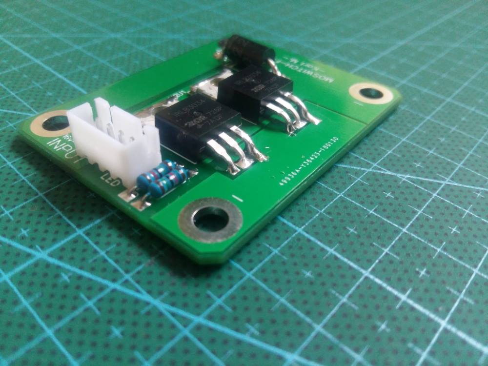
I recently realised, that instead of prefboard soldering i should make a nice looking compact PCB. The board with IRLS3034 (9s) can handle up to 120A (-edit >peak< ) and 80A continuous.
There is also a 60v version (12s) that can do exactly the same, but the fets cost a tiny bit more.
This is the testing of the first PCB-s. I quickly realized that the 2oz copper was not thick enough, so the next ones will have thick solder tracks all across the board.
Here is the “bench test” version with copper pads, i want to over-current test these and push them to their limits:
Yup - do note that these are not for sale, maybe in the future if there is enough interest. This is mainly done because i like to keep my boards looking clean I will probably redesign the whole thing before that happens.
For my use - a 2WD mountainboard that pulls 50A peak per mosfet switch - it’s perfect, maybe if i want to go full crasy on it, the switch shoulde be able to handle it fine. Only 4W of heat is produced in total across all mosfets together @120A - they might get warm if that is continious, but if it is cooled properly i do not see an issue I might even make a really compact 4 mosfet version of this that would be as good as a wire in terms of internal resistance.
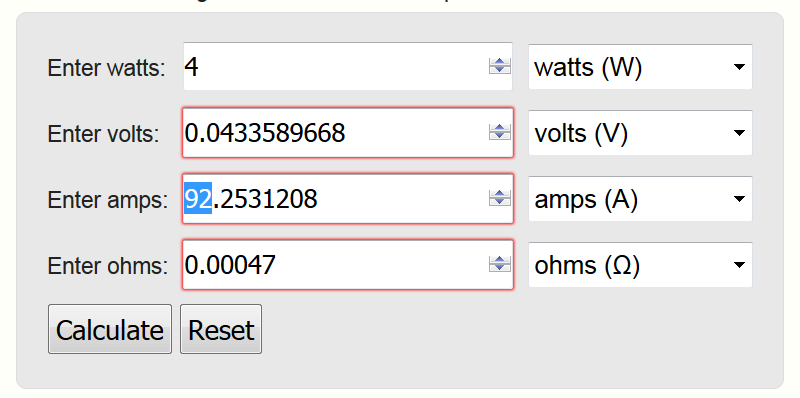
Sorry, i accidentally put in the wrong package name, will fix that. The Mosfets have an internal resistance typ 1.4mOhm, now 3 of these bad boys in parallel will give us 0.47 mOhms, that is 0.00047ohms.
And i do apologize again, i kind of screwed up on the last part - the following was for the @80A when pushing the board to it’s limits (Dual vesc pulls 60A on my board max). I will bench test the board this week and report back actual numbers of amperage and heat with proper graphs.
Silly me, cant even remember what i calculated it for and just put the numbers in. - though i think it should handle 120A if the enclosure is cooled :3 - i have a build log coming up on that.
This is not a sales thread in any way. This just a regular thread - i will update this when i make some progress. I make stuff like this for myself - as i said in a previous reply also.
Remember to account in the temperature co-efficiency of the Rds(on). AKA the resistance will increase with the junction temperature. Although calculating the loss is a bit tedious as the FETs heat up and cool down with changing load, but maybe using just the typical Rds(on) @ 25 C might not be quite realistic.
Absolutely - a good remark. I will be testing the board next week and i will update the main thread with the aquired info. The fets are soldered on to the pcb just like an smd component. The board will help dissipate any excess heat. After all, two of those are perfect for a dual vesc 4.12 build. Since the vesc pulls about 30A per board continious it should work fine. The main key of my project is to keep it low cost and robust.


 - the following was for the